

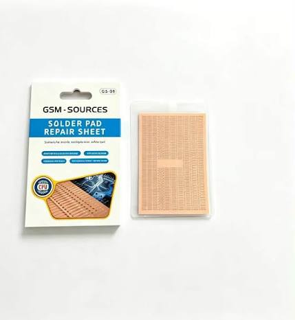
Description
Properties
1.Material: The sheets consist of highly conductive strips of copper with extremely thin layers (of thickness 0.02mm to 0.03mm). This is done to ensure that the strips do not interfere with chip placement on the motherboard.
2.Shapes: The use of copper sheets eliminates the need for technicians to cut and shape conventional jumper wires. The shapes in the sheet include micro-dots (small circles), ovals, and lines leading to dots of various dimensions depending on the diameter of standard BGA pad size.
3.Backed with adhesive: Normally, the BGA pads come on transparent films, and technicians pick the required shapes using fine tweezers.


There are no reviews yet.